New display technologies such as mini-LED, µLED and 3D displays require precisely fitting material and process solutions for the manufacturing of optical elements that influence the light and thus the image information according to the optical layout. This influence can be e.g. light redirection, homogenization, focusing or wavelength conversion. The miniaturization of optical systems is particularly important in the field of augmented reality, virtual reality and mixed reality.
Microoptics
On the material side, the tailoring of property profiles is accomplished by utilizing ORMOCER® technology and nanoparticles, especially quantum dots. The process technology developed at Fraunhofer ISC focuses on the fabrication of complex refractive and diffractive microoptics, e.g. microprisms, index structures and microlenses. In principle, prototyping technologies such as 2PP are used, but the perspective of possible mass production, e.g. by mastering and roll-to-roll imprint, is always kept in mind.

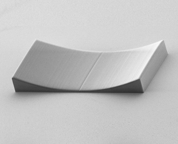
Concave cylindrical microlens with an edge width of approx. 250 µm.
Concrete applications of Fraunhofer technology in the field of displays are:
- (Volume) index structuring e.g. for holography
- Microprism arrays for targeted redirection of light or for light homogenization
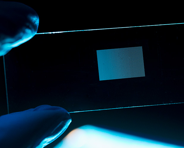
- Microlens arrays of any surface shape and size e.g. for light bundling and/or focusing
- Setups consisting of several layers of microoptics
- Combination with coatings like transparent conductors
Typical specifications:
- Wide range of possible substrates: glass, foils, directly on LEDs, CMOS chips, silicon, ...
- Accuracy: +/- 100 nm
- Roughness: +/- 50 nm
- Typical element sizes: From approx. 1 µm pixel size (diffractive); From approx. 10 µm (refractive)
- Typical areas: Several cm²

