 Center Smart Materials and Adaptive Systems CeSMA
Today’s rapidly growing digital infrastructure demands steadily increasing data rates on all communication platforms.
While optical data transfer is already a standard in the long-haul regime it is still quite rare on the short distance e.g. for chip-to-chip interconnection. Nevertheless, increasing power consumption and strong crosstalk between signal lines imposes limits to conventional electric interconnection technologies also on short length scales. Optical data transfer can overcome these hurdles but technological challenges and expensive integration still impede market penetration of optical interconnects strongly.
Fraunhofer ISC meets the demand for optical data transfer by developing novel core and cladding material systems for conventional optical waveguides. Conventional means here, that core and cladding are fabricated along several subsequent processing steps with UV-lithography. The developed materials are inorganic/organic hybrid polymers (ORMOCER®) that can be tuned to meet application specific requirements and that exhibit extraordinary optical properties and reliability.
3D waveguides written inside optical hybrid polymer (ORMOCER®) using ultrafast laser-based polymerization.
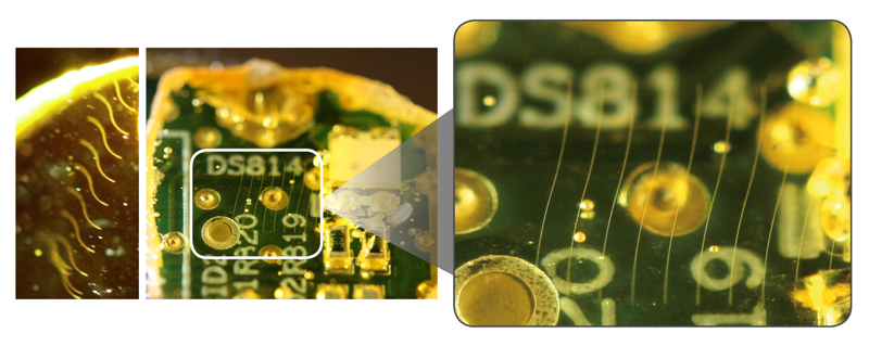
In addition, Fraunhofer ISC develops the materials and the technology for 3D optical interconnects fabricated by ultrashort laser processing. In this process, the waveguide is written along arbitrary trajectories in 3D space to create an optical link between two optoelectronic components, e.g. a VCSEL and a photodiode. This process can be carried out after the assembly of the optical components - hence, no tight tolerances for the assembly. Moreover, the number of processing steps is reduced significantly compared to processing with UV-lithography. This approach has received SPIE’s Green Photonics Award in 2013.