Microfluidic channels and devices are key enablers for lab-on-chip and tissue engineering applications.
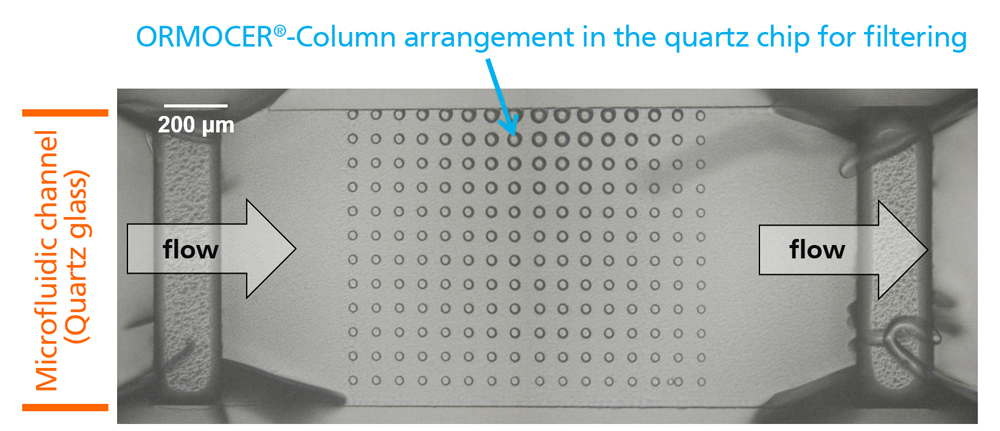
Fraunhofer ISC advances 3D patterning technologies to generate complex functional microfluidic components for tomorrow’s devices. One aspect to this is the fabrication of 3D-channels in glass. Together with Lightfab we explore subtractive manufacturing in e.g. fused silica we are using ultrashort laser pulses. The process flow, i.e. scanning exposure of the desired structure inside the volume of a glass substrate and subsequent etching for the removal of exposed regions, enables the manufacturing of 3D parts directly from computer design. This process called selective laser etching (SLE) enables feature sizes as small as 10 µm.
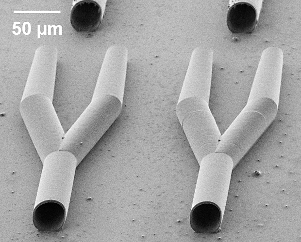
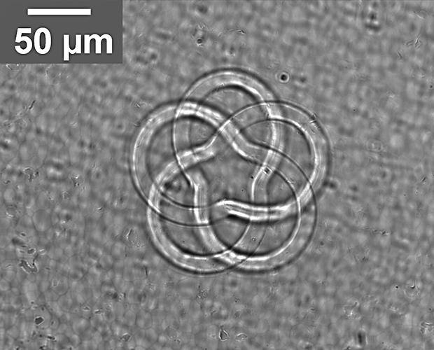
An alternative way to create microfluidic channels is two-photon polymerization (2PP), which is an additive process with a resolution down to 100 nm. Similar the SLE an ultrafast laser is scanned in 3D space to solidify polymer along its path. This allows the generation of arbitrary 3D microstructures, particularly tiny channels and devices. 2PP can also be conducted inside SLE-written channels which opens up the way to even more sophisticated microfluidic or optofluidic devices.


